LNBD

Nanomaterial-based Devices

The LNBD develops and employs different nanomaterials, such as metal nanoparticles, poly aromatic hydrocarbons, silicon nanowires and carbon nanotubes, in a variety of electronic devices. Control over the size, shape, structure and morphology of such nanospecies enables the design of complex sensing functions that can address practical requirements from sensing platforms. In addition, both fabrication using bottom-up wet chemistry approaches, and the utilization of organic material coatings are simple. This enables the use of nanomaterials for different applications. The LNBD focuses on the following applications:

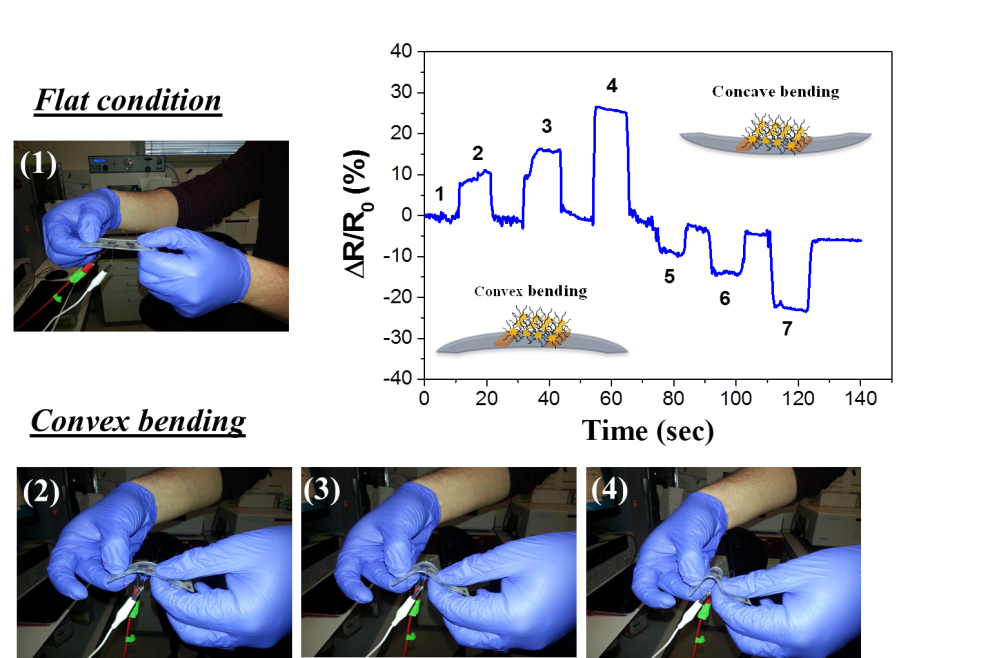
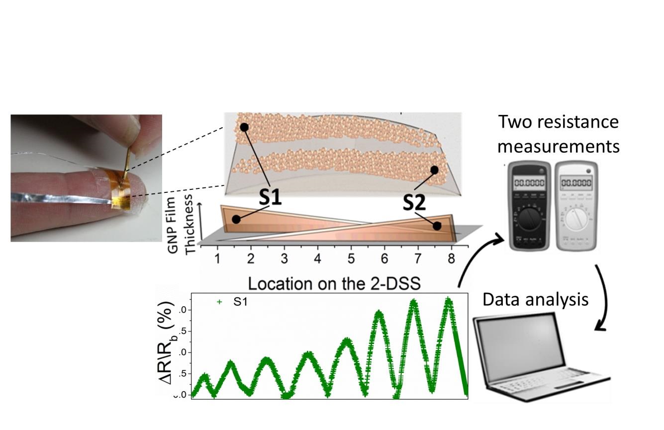
Nanomaterial-based sensors: R&D for use in artificially intelligent nanoarray and electronic skin applications.

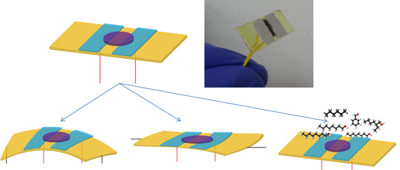
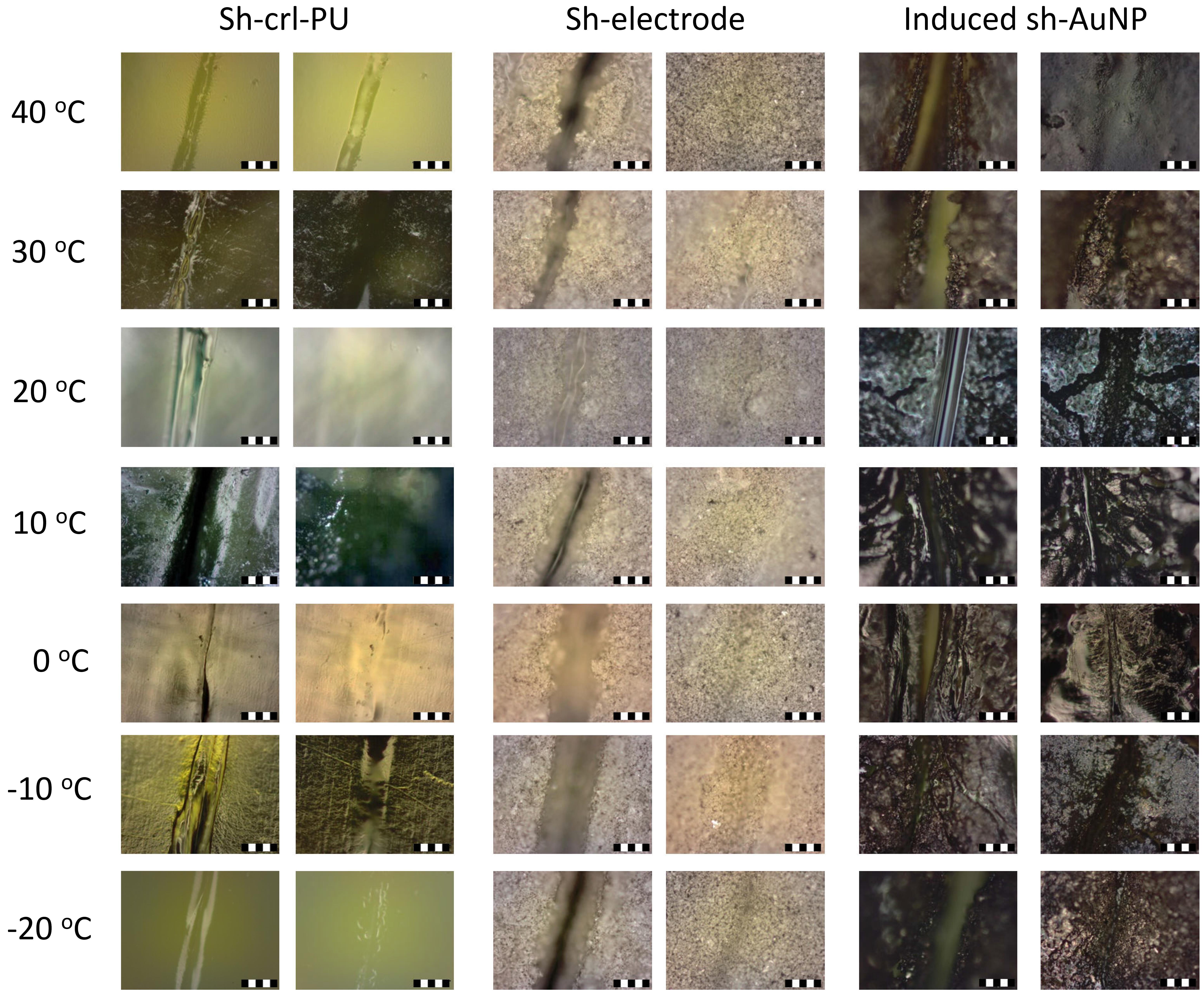
Self-healing sensors: development of electronic sensors with engineered structures that enable self-repair and full functionality following mechanically destructive damage.

Printed electronics:  development of new printing and self-assembly techniques that enable the optimal implementation of nanomaterials in electronic devices.

Nanomaterial-based Sensors

LNBD research combines knowledge from multi-disciplinary fields (microelectronics, nanotechnology, microfluidics, machine learning, biochemistry, medicine, genetics) in developing novel nanomaterials based on solid-state and flexible sensors, as well as electronic sensor nanoarrays for applications in healthcare diagnosis, consumer electronics, robotics, sports and fitness, environmental monitoring and other areas. These sensors are based on either resistive films of metal nanoparticles, carbon nanotubes (CNT) or poly-aromatic hydrocarbons (PAH) or on chemical field effect transistors (chem-FETs) based on Si nanowires or single-walled CNTs.

The devices’ nanoscale size offers several advantages, such as large surface-to-volume ratio and unique chemical, optical, and electrical properties. The increased surface area of the nanomaterials provides highly active interfaces, increased sensitivity and lowered response and recovery times. Additionally, the nanoscale size makes these materials sensitive to localized entities of similar size, from small molecules to large macromolecules. Combined with machine learning approaches and specialized calibration algorithms, such electronic sensory nanoarrays can serve as substitutes for biological sensory systems.

Figure 1. Present and future applications for flexible sensors; the middle image shows a flexible sensor. (a) An analog resistive touch screen with a simple mechanical switch mechanism to locate a touch. (b) E-skin based on flexible sensors for present robotic applications. The upper image shows the da Vinci Surgical System, the most widely used robotic surgical system in the world. The lower image shows a three fingered gripper. (c) E-skin that could in the future provide a natural sense of touch to prosthetic limbs. (d) Wearable sensors for monitoring an individual's physical parameters like movement, respiratory rate and heart rate while exercising. (e) Large-area flexible sensing systems composed of a large number of individual sensors for early detection of cracks in large structures such as aircrafts or buildings. (f) Printed sensors for future space applications.

Self-healing Sensors

The LNBD is focusing efforts on the development of self-healing electronic sensory nanoarrays that will have the ability to repair themselves and gain back full functionality after undergoing mechanical damage caused by usage over time. Towards this end, a new self-healing elastomer and its composite are fabricated together with a sensing layer. The sensitivity of these self-healing sensors to pressure and strain is highly comparable to ordinary human or electronic skin. The same self-healing device can serve as sensor for gas analytes, thus opening a door for wider spectrum of important applications.

Printed Electronics

The realization of new inexpensive and robust printing and self-assembly techniques that implement nanomaterials in electronic devices and sensors promises to bring about revolutionary advances in manufacturing.

The LNBD is committed to the development of new manufacturing processes and adaptation/extension of conventional printing methods (such as inkjet) for printed nanomaterial electronic devices. The lab has developed a new direct-write printing method for patterning nanometeric species in addressable locations by means of evaporative deposition from a propelled anti-pinning ink droplet (PAPID), in a manner analogous to a snail trail.

This approach achieves continuous patterns that can be formed on rigid or flexible substrates, even within 3D concave closed shapes. It also enables production of a controlled thickness gradient along the length of the patterns.

Additionally, lab researchers have developed a simple and efficient method for the deposition of highly ordered and aligned nanowire arrays on a wide range of substrates, including silicon, glass, metals, and flexible plastics, based on spray-coating of a nanowire suspension under controlled conditions. These versatile, low-cost printing approaches can produce a wide range of unusual electronic systems not achievable with other methods.

Schematic of the spray-coating process that involves a direct transfer of NW suspension to the receiver substrates. (A) Schematic and scanning electron microscopy (SEM) image of the NW sample used in this study. (B) Schematic of the NW suspension. (C) Schematic of the assembled apparatus used in this study. (D) Schematic and optical microscopy image of Si NW spray-coated on the SiOx/Si substrate.